
Jong Hoon

“Ideally one would desire an indefinitely large memory capacity such that any particular… word would be immediately available… We are… forced to recognize the possibility of constructing a hierarchy of memories each of which has greater capacity than the preceding but which is less quickly accessible.”
– A. W. Burks, H. H. Goldstine, and J. von Neumann, Preliminary Discussion of the Logical Design of an Electronic Computing Instrument (1946).
In this post, I summarize Chapter 2—Memory Hierarchy Design—from Computer Architecture: A Quantitative Approach by Patterson and Hennessy.
Introduction to Memory Hierarchy
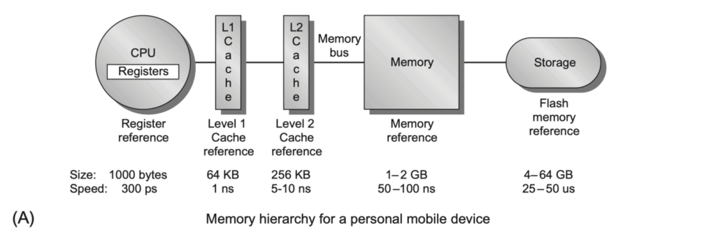
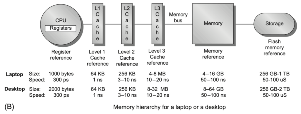
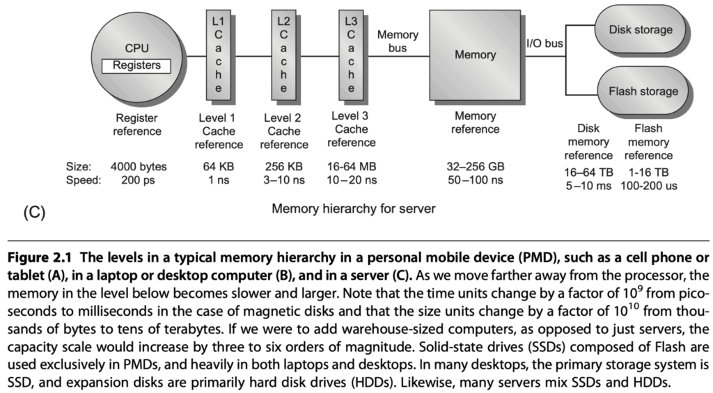
Modern computer systems aim to balance performance and cost in the face of inherent memory limitations. Ideally, a system would have unlimited fast memory, but this is not practically achievable due to cost, power, and physical constraints. Instead, architects build a memory hierarchy that optimizes for access time, bandwidth, and efficiency.
Core Ideas of Memory Hierarchy
- The design of memory systems takes advantage of the principle of locality:
- Temporal locality: Recently accessed data is likely to be used again soon.
- Spatial locality: Data near recently accessed addresses is likely to be used soon.
- These allow for non-uniform memory access patterns that are still predictable.
- The hierarchy exploits cost-performance trade-offs in memory technologies:
- Fast memory (e.g., SRAM) is expensive per byte.
- Cheap memory (e.g., DRAM, SSD) is slower.
- Goal: Create a system that is:
- Almost as cheap as the lowest-cost memory.
- Almost as fast as the fastest memory.
Inclusion Property
- In most hierarchies, lower levels (like L3 or main memory) contain all the data from higher levels (L1/L2).
- This inclusion property simplifies consistency and coherency management, though it is not universal.
The Performance Gap Problem
- Since 1980, the performance of processors has dramatically outpaced memory latency improvements.
- This growing gap makes efficient memory hierarchy design crucial.
- For example, in 2017, companies like AMD, Intel, and NVIDIA began deploying High Bandwidth Memory (HBM) to reduce this gap.
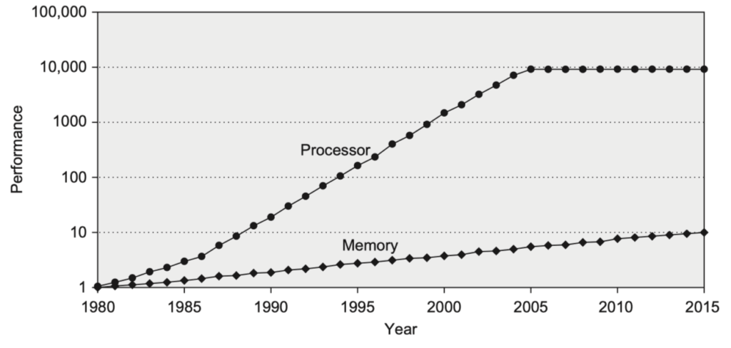
Figure 2.2. Starting with 1980 performance as a baseline, the gap in performance, measured as the difference in the time between processor memory requests (for a single processor or core) and the latency of a DRAM access (assuming a single DRAM and a single memory bank), is plotted over time. In mid-2017, AMD, Intel and Nvidia all announced chip sets using versions of HBM technology.
Bandwidth Demands in Multicore Systems
Consider the Intel Core i7-6700 as a real-world case:
- Each core generates two memory references per core-cycle
- With 4 cores at 4.2 GHz:
- 32.8 billion 64-bit data refs/sec = ~244 GB/sec
- 12.8 billion 128-bit instruction refs/sec = ~191 GB/sec
- Total theoretical demand: Over 400 GiB/sec
- Actual DRAM bandwidth is much lower: ~32.1 GiB/sec
- The memory system must bridge this massive bandwidth mismatch.
Hardware Solutions to Bandwidth and Latency
- Multi-porting and pipelining of caches
- Three-level cache hierarchy:
- Private L1 & L2 per core
- Shared L3
- Some systems include L4 DRAM caches (stacked or embedded DRAM)
- Split L1 for instruction and data
Design Focus Areas
Designers aim to optimize:
- Average Memory Access Time (AMAT)
- Cache access time
- Miss rate
- Miss penalty
- Power consumption:
- Static power (leakage)
- Dynamic power (access, switching)
Basics of Memory Hierarchies: A Quick Review
- Cache Concepts:
- Hit / Miss, Block/Line, Tag
- Spatial & Temporal Locality
- Set associativity:
- Direct-mapped, n-way set associative, Fully-associative
- Write Policies:
- Write-through: Write to memory on every store
- Write-back: Write to memory only when evicted
- Write buffers: Hide write latency
- Three Cs of Misses:
- Compulsory: First access to a block
- Capacity: Cache can’t hold all active data
- Conflict: Limited associativity causes evictions
- 4th C: Coherency – Arises in multithreaded/multicore systems
- Covered in Chapter 5, “Multiprocessors and Thread-Level Parallelism”
- Misses per instruction is a better measure than miss rate alone

-
Best metric: Average Memory Access Time (AMAT)

Latency Tolerance Techniques
Modern processors use various techniques to hide or tolerate memory latency:
- Speculative execution
- Multithreading
Six Key Cache Optimizations
- Larger block size – reduces compulsory misses
- Bigger caches – reduces capacity misses
- Higher associativity – reduces conflict misses
- Multi-level caches – hides miss penalty from higher levels
- Prioritizing read misses over writes – improves perceived performance, often by using write buffers that support non-blocking stores and mitigate RAW hazards by forwarding data from the buffer.
- Avoid address translation (e.g., TLB lookups) during cache indexing to reduce hit time
Memory Technology and Optimization
Modern memory systems aim to balance latency, bandwidth, power, and cost. This section reviews the underlying memory technologies and key architectural strategies for improving memory performance.
Memory Latency Metrics
- Access Time: Time from sending a read request to when the data arrives.
- Cycle Time: Minimum time between two independent memory requests.
1. SRAM Technology
Static RAM (SRAM) is fast, does not require refresh, and has nearly equal access and cycle times.
- Structure: 6 transistors per bit.
- Usage: Typically used for caches.
- Previously in separate chips.
- Now implemented as on-chip memory, e.g., up to 60MB shared cache for 24-core CPUs.
Typical Cache Access Latency and Capacity (Server Scale):
| Level | Access Time | Size |
|---|---|---|
| L1 | ~1 ns | ~64 KB |
| L2 | 3–10 ns | ~256 KB |
| L3 | 10–20 ns | ~16–64 MB |
| DRAM | 50–100 ns | 32–256 GB |
Why Larger Caches Are Slower and Power-Hungry:
- Access time ∝ number of blocks (except hit detection and selection in a set associative cache)
- Static power ∝ number of bits
- Dynamic power ∝ number of blocks
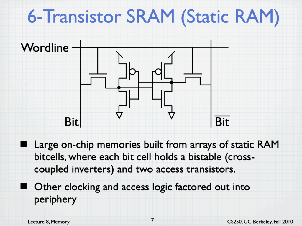
Six-transistor SRAM from UC Berkeley Lecture
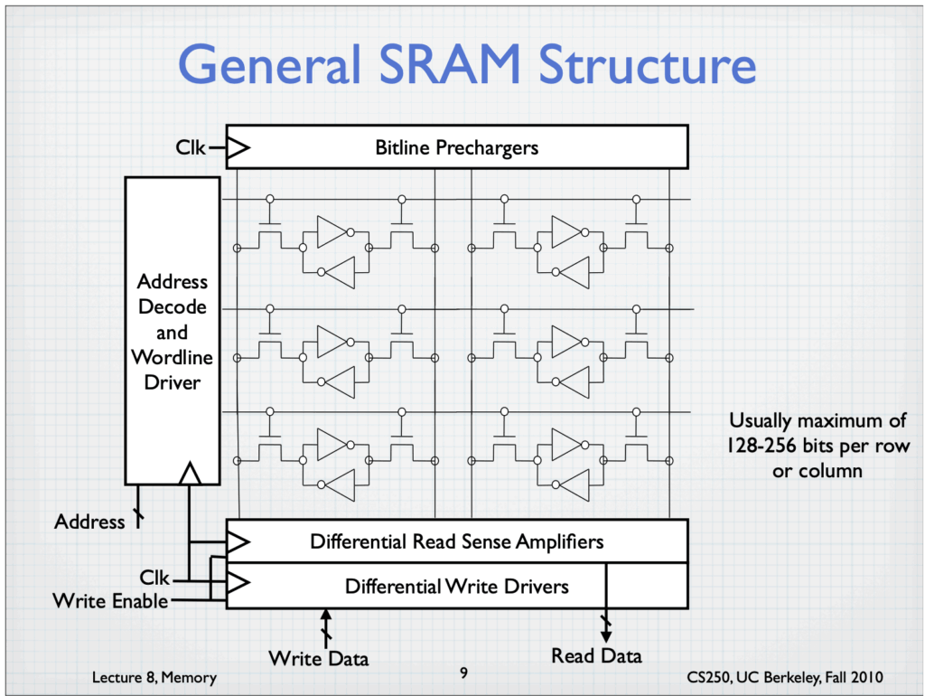
General SRAM structure from UC Berkeley Lecture
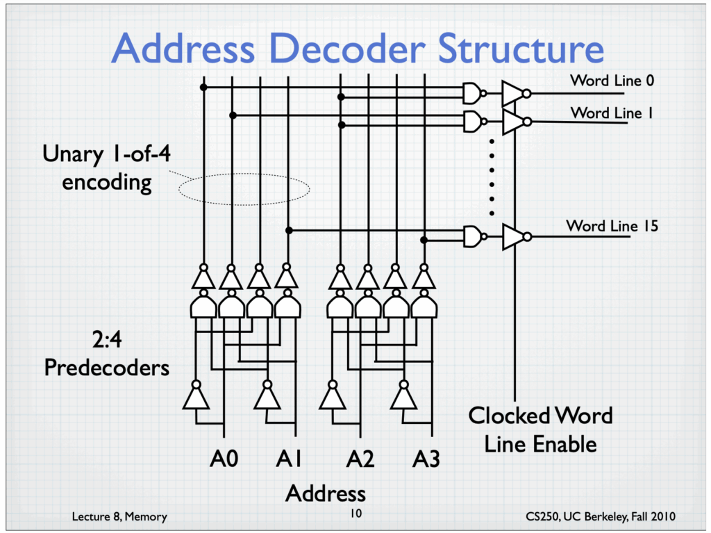
Address decoder structure from UC Berkeley Lecture
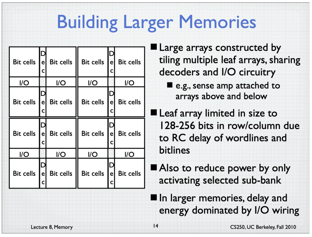
Building larger memories from UC Berkeley Lecture
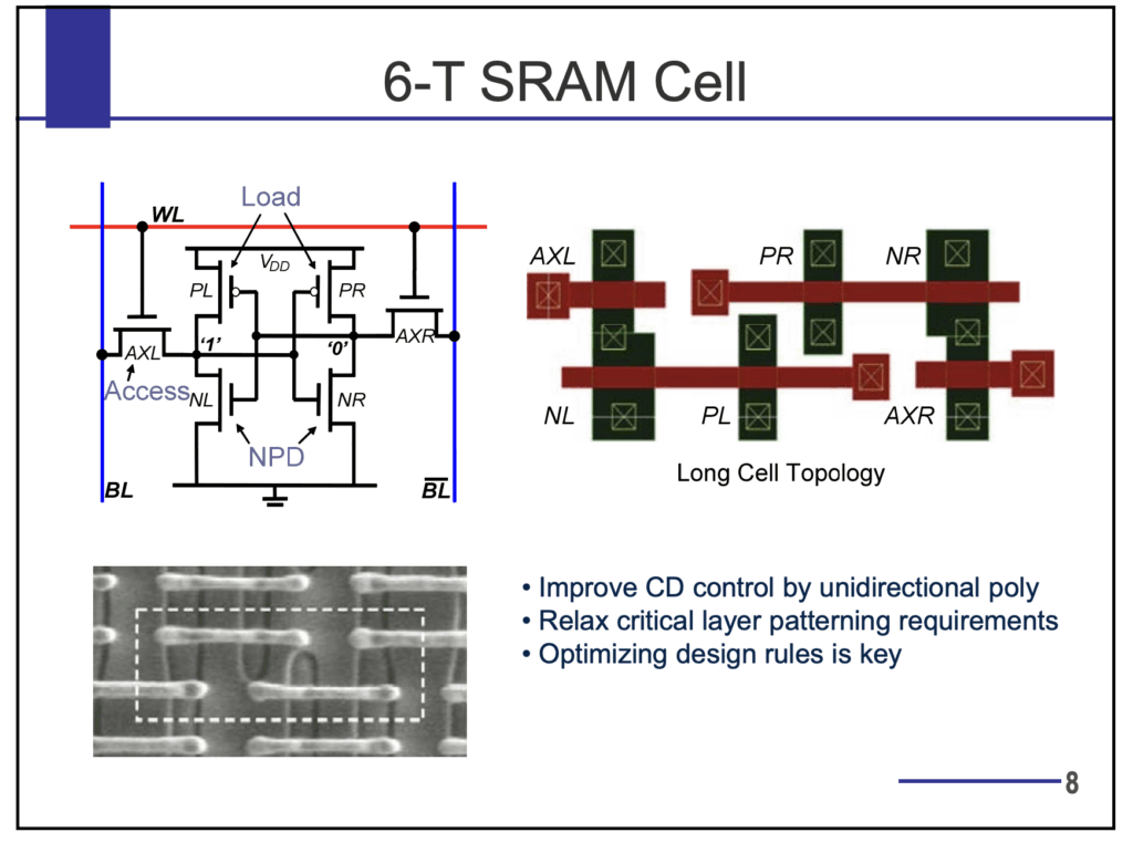
6T SRAM Cell from UC Berkeley Lecture
2. DRAM Technology
Dynamic RAM (DRAM) uses capacitors and requires regular refreshing.
- 1 transistor + 1 capacitor per bit
- Sensing half high charge = 1
- Sensing half low charge = 0
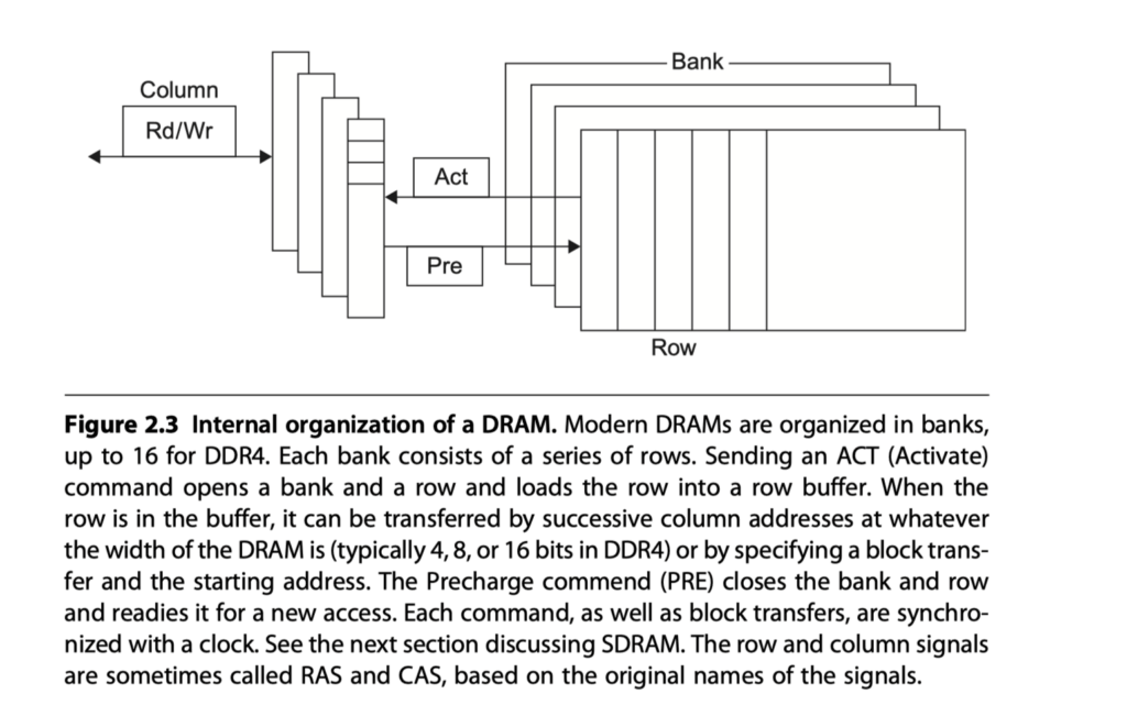
- Addressing: Split into two stages
- The first half of the address: RAS (Row Access Strobe) for row
- The other half: CAS (Column Access Strobe) for column
- Reading:
- Accessing a row (RAS) in DRAM loads it into a row buffer, after which CAS signals select the desired columns to be read.
- Reading a row destroys its content, which must be written back if not used
- Refreshing:
- To maintain data integrity, DRAM cells must periodically refill the charges that naturally leak over time.
- This occurs once every 64 ms and consumes less than 5% of total memory access time.
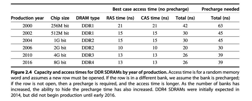
3. Improving DRAM Performance: SDRAMs
Synchronous DRAM (SDRAM) improves coordination with memory controllers using a clock signal, while previous version of DRAMs worked asynchronously so that they had overhead to synchronize with the controllers.
- Burst transfer mode allows multiple words to be accessed per request
- More bandwidth with wider DRAM interfaces, such as 4-bit, 8-bit, or 16-bit buses in DDR2 and DDR3, help increase memory bandwidth.
- DDR (Double Data Rate) DRAM transfers data on both rising and falling clock edges
- Multiple banks enable:
- Interleaved and overlapped access to different banks
- Improved access time
- Better power management
- Address = Bank number + Row address + Column address
- Access Steps in SDRAMs:
- When accessing DRAM, the memory controller first activates a bank and a specific row (via the Row Address Strobe, or RAS),
- followed by the column address to select the desired data.
- Depending on the request, the system may read a single item or initiate a burst transfer for multiple items.
- Pre-charge operation
- After accessing a row, the DRAM requires a pre-charge operation to close the current row before accessing another row in the same bank, which introduces a pre-charge delay.
- However, if subsequent accesses target different rows in different banks, they can be overlapped, avoiding this delay and improving memory throughput.
- DIMMs (Dual Inline Memory Modules) group 4–16 DRAM chips
- Typical width: 8 bytes + ECC
- Power Saving Techniques:
- Lower voltages (e.g., 1.2V in DDR4)
- Multi-bank: Only one row active per bank
- Power-down mode (clock gated except for refresh)
4. Graphics DRAMs (GDDR)
Graphics DRAMs, special class of DRAMs based on SDRAM designs, are optimized for bandwidth, not latency.
- GDDR5 design is based on DDR3
- Wider interface (32-bit vs. 4, 8, 16-bit typical designs)
- Directly soldered to GPU (not expandable)
- 2–5× bandwidth vs DDR3
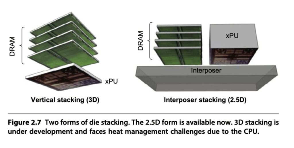
5. Packaging Innovation: HBM
High Bandwidth Memory (HBM) integrates DRAM closely with compute chips.
- Stacked or embedded DRAM in the same package
- Lower latency
- Higher bandwidth
- Successor to GDDR5
Packaging Techniques:
- 3D Stacking
- DRAM dies on top of CPU die using solder bumps
- Requires heat dissipation
- e.g., 8 chips, 8 GiB, 1 TB/s
- 2.5D Stacking
- DRAM stacked on interposer substrate
- Less thermal coupling, still high BW
6. Flash Memory
Flash is a form of non-volatile EEPROM.
- NAND Flash is higher density than NOR Flash
- Drawbacks:
- Sequential access (vs. random)
- Slow writes (erase-before-write, block-level erasure)
Flash vs DRAM:
| Feature | Flash | DRAM |
|---|---|---|
| Read Latency (2 KiB) | ~75 µs
(300× faster than HDD) |
~500 ns
(150× faster than Flash) |
| Write Latency | 1500× DRAM
(Erase before overwrite) |
Fast |
| Nonvolatile | Yes | No |
| Write cycles | ~100,000 | Unlimited |
| Cost | ~10× cheaper | More expensive |
Flash Controller Responsibilities:
- Redundant block mapping
- Page-level transfer and caching
- Write leveling (to extend lifespan)
7. Phase-Change Memory (PCM)
Phase-change memory uses heat to switch between crystalline and amorphous states.
- Each bit = 2D crosspoint (memristor)
- Read: Measure resistance
- Write: Apply current to change phase
Intel & Micron’s XPoint memory (2017) offered:
- Much better write endurance than Flash
- 2–3× faster reads
8. Enhancing Memory System Dependability
Memory errors can be hard (permanent) or soft (transient).
ECC and Protection:
- I$ (Instruction cache) → Parity bit only
- D$ + Main Memory → Error Correction Code (ECC)
- Typical overhead: 1 ECC bit per 8 data bits (e.g., 64-bit word → 8 ECC bits)
Chipkill:
- Redundant ECC scheme similar to RAID
- Can recover from entire chip failure
- Used in IBM, SUN, Google clusters
- Intel calls it SDDC
Example Error Rates (10,000 nodes, 4GiB each):
| Protection | Unrecoverable Errors |
|---|---|
| Parity Only | Every ~17 minutes |
| ECC Only | Every ~7.5 hours |
| Chipkill | Every ~2 months |
Reference
- Chapter 2 in Computer Architecture A Quantitative Approach (6th) by Hennessy and Patterson (2017)
- CS250 VLSI Systems Design Lecture 8: Memory by John Wawrzynek, Krste Asanovic, with John Lazzaro and Yunsup Lee (TA), CS250, UC Berkeley, Fall 2010
- EE241 – Spring 2011 Advanced Digital Integrated Circuits Lecture 9: SRAM